Semiconductor & Wafer
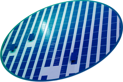
Provides 3D measurement sensors for wafers
and semiconductor-related products
and semiconductor-related products
Semiconductor manufacturers are continuing to innovate the process
of miniaturizing integrated circuits. As chip miniaturization
and thinning become possible, fine shape measurement technology requires in the chip manufacturing process. In addition, a multi-stage lamination process of high-capacity
thin film wafers is essential, and the demand for wafer bending inspection
is increasing significantly.
Nexensor uses optical interference source technology to provide
3D measurement sensors for wafers and semiconductor-related products.
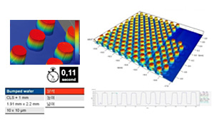
Micro Bump Height
Wafer (silicon, sapphire)
thickness measurement
thickness measurement
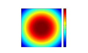
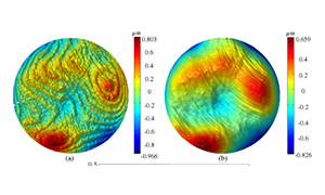
Wafer surface inspection
and shape measurement
and shape measurement
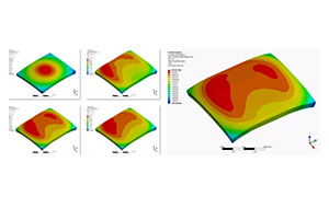
Warpage, thickness, roughness,
microstructure shape
measurement of FoWLP
microstructure shape
measurement of FoWLP